The Carbon Neutral Circuit: Designing Sustainable PCB Packaging for a Circular EconomyAuthor : Adrian September 17, 2025Table of ContentsIn a world increasingly focused on sustainability, how can the electronics industry reduce its environmental impact? One key area of focus is sustainable PCB packaging, which plays a vital role in achieving a circular economy. By prioritizing circular economy PCB packaging, reducing carbon footprint in PCB packaging, and embracing concepts like life cycle assessment and cradle to cradle design, manufacturers can minimize waste and promote eco-friendly practices. In this blog, we’ll dive deep into how sustainable PCB disposal and innovative packaging solutions can help build a greener future for the electronics industry.
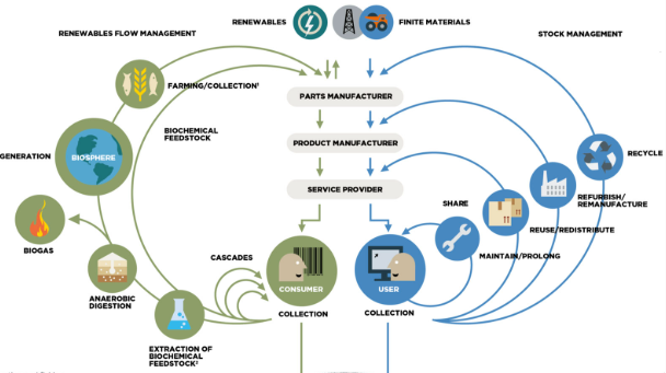
Why Sustainable PCB Packaging Matters in a Circular EconomyThe concept of a circular economy is simple: instead of the traditional "take-make-waste" model, we aim to reuse, recycle, and repurpose materials to keep them in circulation. For printed circuit boards (PCBs), which are at the heart of nearly every electronic device, packaging plays a critical role in this process. PCB packaging not only protects components during transport but also contributes significantly to the overall environmental footprint of electronics manufacturing. Traditional PCB packaging often relies on single-use plastics and non-recyclable materials, which end up in landfills or as pollution. By focusing on circular economy PCB packaging, the industry can reduce waste, lower carbon emissions, and conserve valuable resources. Sustainable packaging solutions also align with growing regulatory demands and consumer expectations for greener practices.
Reducing Carbon Footprint in PCB Packaging: Key StrategiesReducing the carbon footprint of PCB packaging is a critical step toward sustainability. The production, transportation, and disposal of packaging materials all contribute to greenhouse gas emissions. Here are some actionable strategies to minimize this impact:
By integrating these practices, companies can make significant strides in reducing carbon footprint in PCB packaging, contributing to a more sustainable supply chain.
Life Cycle Assessment for PCB Packaging: Understanding the Full ImpactA life cycle assessment (LCA) for PCB packaging is a powerful tool to evaluate the environmental impact of a product from cradle to grave. This method analyzes every stage of the packaging’s life, including raw material extraction, production, use, and disposal. Conducting an LCA helps identify areas where improvements can be made to reduce environmental harm. For example, an LCA might reveal that the energy-intensive production of plastic packaging contributes 60% of its total carbon emissions. Armed with this data, manufacturers can switch to materials like recycled paper, which may cut emissions by half during production. Additionally, an LCA can highlight the benefits of reusable packaging systems, showing how they reduce waste by up to 70% over single-use options. Implementing life cycle assessment for PCB packaging ensures that decisions are based on hard data, leading to more sustainable outcomes. It also helps companies comply with regulations and build trust with environmentally conscious customers who value transparency. Cradle to Cradle PCB Packaging: Designing for Reuse and RecyclingThe cradle to cradle (C2C) design philosophy takes sustainability a step further by ensuring that products are designed with their entire life cycle in mind. For PCB packaging, this means creating materials that can be reused or recycled indefinitely without losing value. Unlike the traditional "cradle to grave" model, cradle to cradle PCB packaging focuses on eliminating waste altogether. One example of C2C in action is the use of biodegradable packaging materials that break down naturally without releasing toxic substances. Another approach is modular packaging designs that allow components to be reused for multiple shipments. For instance, a reusable PCB tray system could reduce packaging waste by 80% over five cycles of use, based on industry estimates. Additionally, C2C encourages the use of non-toxic adhesives and coatings in packaging to ensure that materials can be safely recycled. By designing for disassembly, manufacturers make it easier to separate components at the end of their life, promoting a truly circular economy.
Sustainable PCB Disposal: Closing the LoopDisposal is often the most overlooked aspect of PCB packaging, yet it’s a crucial part of achieving a circular economy. Sustainable PCB disposal involves ensuring that packaging materials are either recycled, composted, or repurposed rather than sent to landfills. Here’s how this can be achieved:
Sustainable PCB disposal not only reduces landfill waste but also conserves resources by reintroducing materials into the production cycle. It’s a vital step in closing the loop of a circular economy. Challenges in Implementing Sustainable PCB PackagingWhile the benefits of sustainable PCB packaging are clear, there are challenges to overcome. Cost is often a significant barrier, as eco-friendly materials like bioplastics can be 20-30% more expensive than traditional plastics. Additionally, the infrastructure for recycling or composting may not be widely available in all regions, limiting the effectiveness of sustainable disposal practices. Another challenge is balancing sustainability with functionality. PCB packaging must protect delicate components from static, moisture, and physical damage. Finding eco-friendly materials that meet these strict requirements can be difficult, though innovations like biodegradable anti-static films are beginning to bridge this gap. Finally, regulatory differences across countries can complicate global supply chains. What’s considered recyclable in one region might be treated as waste in another. Harmonizing standards and investing in research for universal solutions will be key to overcoming these hurdles.
Innovations Driving Sustainable PCB PackagingThe good news is that technology and innovation are paving the way for more sustainable PCB packaging. Here are a few exciting developments:
These innovations show that sustainability and performance can go hand in hand, offering hope for a carbon-neutral future in PCB packaging. How Manufacturers Can Transition to Circular Economy PracticesTransitioning to circular economy PCB packaging requires a strategic approach. Manufacturers can start by conducting a baseline assessment of their current packaging processes to identify high-impact areas for improvement. Partnering with suppliers who prioritize sustainability can ensure a steady supply of eco-friendly materials. Investing in employee training is also essential. Educating staff on sustainable practices, from design to disposal, ensures that everyone is aligned with the company’s green goals. Finally, transparency with customers about sustainability efforts can build trust and loyalty, as more than 70% of consumers prefer to support environmentally responsible brands, according to recent surveys.
The Future of Sustainable PCB PackagingThe journey toward a carbon-neutral circuit is just beginning, but the momentum is undeniable. As regulations tighten and consumer demand for sustainability grows, the electronics industry must continue to innovate in circular economy PCB packaging. By focusing on reducing carbon footprint in PCB packaging, embracing life cycle assessment, adopting cradle to cradle principles, and prioritizing sustainable PCB disposal, manufacturers can lead the way in building a greener future. At every step, from design to disposal, there are opportunities to make a difference. Sustainable PCB packaging isn’t just a trend—it’s a necessity for preserving our planet for future generations. With the right strategies and innovations, the industry can close the loop and achieve a truly circular economy. Share · · · · The Role of Flux in PCB Wave Soldering: Selection, Application, and Residue RemovalMarch 16, 2026PCB wave soldering flux types include rosin, water-soluble, and no-clean options with varying activity levels for oxide removal and solder flow. This guide covers selection criteria, spray foam drop-jet application methods, residue removal processes, and alternatives like nitrogen blanketing to boost joint reliability and yields for engineers. Article Achieving Uniform Solder Fillets in PCB Wave Soldering: Process ControlMarch 16, 2026Achieve uniform solder fillets in PCB wave soldering with process control strategies. Optimize flux, preheat, wave height, conveyor speed for consistent fillet shape, height, and wetting balance. Includes visual inspection tips and troubleshooting for reliable through-hole assemblies. Boost quality in production. Article Optimizing Conveyor Speed for Efficient PCB Wave SolderingMarch 16, 2026Learn PCB wave soldering conveyor speed calculation to manage dwell time, immersion depth, and throughput effectively. Electric engineers get practical steps, best practices, and troubleshooting tips for higher process efficiency and fewer defects in wave soldering operations. Article Understanding IPC Standards for PCB Surface Finishes: Ensuring Quality and ComplianceMarch 11, 2026Understand IPC standards IPC 4552 ENIG and IPC 4553 immersion silver for PCB surface finishes. Ensure compliance, enhance solderability, and prevent common defects to achieve reliable, high quality circuit boards. Article Miniaturization Challenges in PCB AssemblyMarch 11, 2026Navigate the complexities of high density interconnect PCB assembly and precise component placement. Learn to tackle miniaturization challenges, from tiny part handling to thermal stress, ensuring robust and reliable electronics. Article High Speed Routing Techniques: PCBMarch 11, 2026Master high speed routing in PCBs to ensure signal integrity and minimize electromagnetic interference. Learn essential techniques for robust designs, from controlled impedance to differential pair strategies. Prevent performance issues and achieve reliable electronics. ArticleGet Instant PCB |